TECHNICAL

μ-Amp Technical Details

A practical description of the circuit, board, controls and current specifications. This page is set up so measured performance data can be added later as testing is completed.

PRELIMINARY SPECIFICATIONS

The circuit at a glance

These are the current design details. Additional measured specifications can be added as production testing is completed.

PurposeCompact onboard guitar preamplifier / booster
Active deviceNE5534 single audio operational amplifier
PowerStandard 9 V battery
Battery switchingStereo output jack disconnects battery negative when the guitar cable is removed
Control500 kΩ off-board potentiometer
BypassDPDT effect / bypass switching
PCB connections15 numbered edge pads
Wiring optionsPCB link traces or direct point-to-point wiring for the paired off-board connections
Nominal gain rangeApproximately 0× to 4.2× (about +12 dB maximum), based on the present circuit arrangement

SIGNAL PATH

How the audio moves through the μ-Amp

The guitar signal enters through the effect side of the DPDT switch, passes through the input network and into the NE5534 amplifier stage. The 500 kΩ control is part of the amplifier feedback arrangement and controls the amount of boost.

The amplified signal is AC-coupled to the output side of the bypass switch and then to the guitar's output jack.

POWER

9 V operation

The circuit operates from a standard 9 V battery. The output jack uses its Ring contact as the battery-negative switch, so unplugging the guitar cable disconnects the battery.

The board's ground connects to the jack Sleeve.

BYPASS

Effect and direct signal paths

The DPDT switch changes both the input and output sides at the same time. In the effect position, the pickup signal is routed through the μ-Amp. In bypass, the input is connected directly to the output path.

The PCB includes link traces for Pads 1–2, 9–10, 11–12 and 14–15. Those connections may instead be made directly between the off-board parts.

BOARD

Installer-oriented PCB

Large numbered pads around the perimeter give clear wiring points for the external switch, control, battery and output jack. The board is supplied preassembled in the completed versions.

  • 15 numbered connection pads
  • Through-hole construction
  • NE5534 in an 8-pin DIP package
  • Off-board potentiometer, DPDT switch, stereo jack and battery

MODELED PERFORMANCE

What the circuit model predicts

These plots were made from the present circuit values and simple operating assumptions to show how the μ-Amp should behave as the control is advanced.

Important: These are analytical / simulation-style approximations, not production test measurements. Several graphs deliberately state assumptions such as available output headroom, supply voltage, load resistance, or a soft-clipping model. Measured specifications can be added separately when bench testing is completed.

Gain, control position and headroom

The first group shows how increasing the 500 kΩ control raises the modeled gain, while the maximum input level that can remain unclipped falls as gain increases.
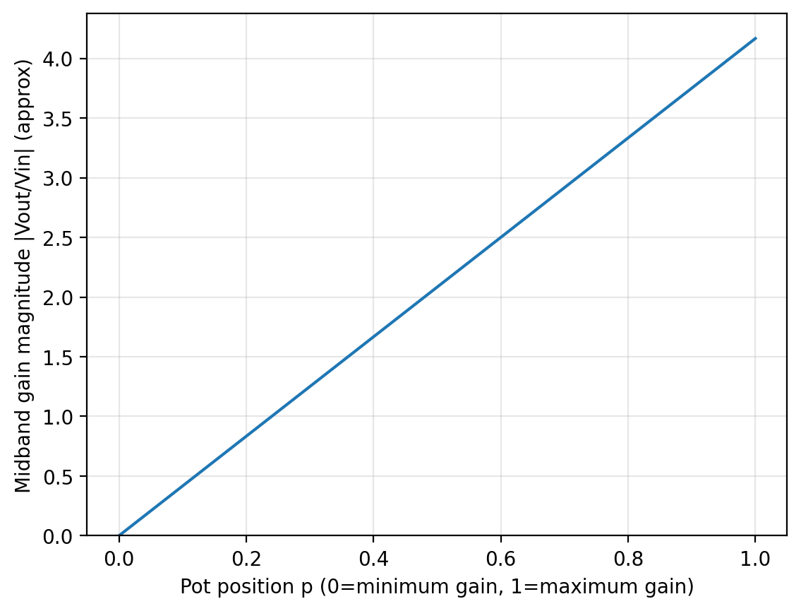
Modeled linear gain versus pot position
Gain versus control position With pot position normalized from 0 to 1, the simple resistor-ratio model rises almost linearly and reaches about 4.17× at full setting.
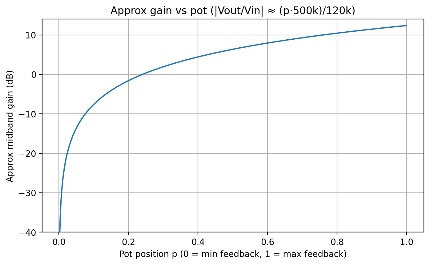
Modeled gain in decibels versus pot position
The same gain shown in decibels The logarithmic dB scale makes the low end appear much steeper. Full modeled gain of about 4.17× corresponds to roughly +12.4 dB.
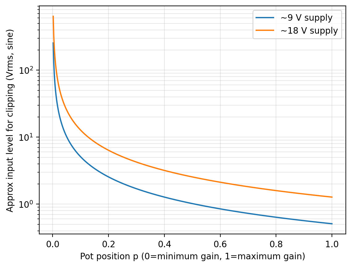
Approximate RMS input clipping threshold versus pot position
Approximate input level at clipping This graph expresses the limit as sine-wave RMS input voltage. As boost is increased, a smaller input signal is enough to reach the assumed output-voltage limit. The two curves compare the stated 9 V and 18 V headroom assumptions.
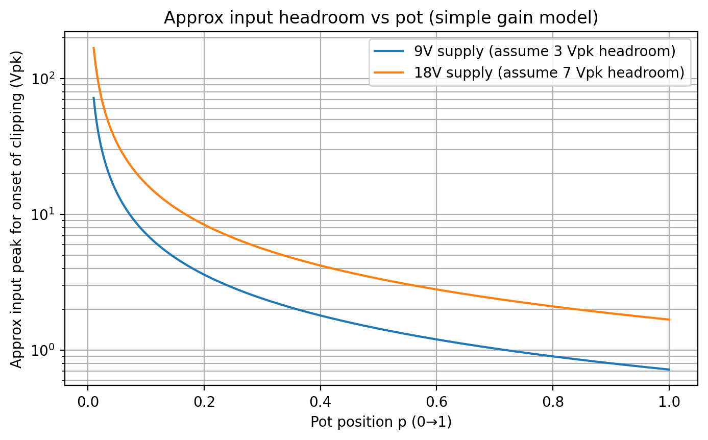
Approximate peak input headroom versus pot position
Input headroom versus control position This is the same general idea expressed as input peak voltage. The 9 V curve assumes about 3 V peak of usable output headroom; the 18 V curve assumes about 7 V peak.

Compression, clipping and transfer shape

These plots use a deliberately simple soft-clipping model. They are useful for visualizing the trend: larger signals and higher boost move the circuit progressively farther away from an ideal straight-line amplifier.
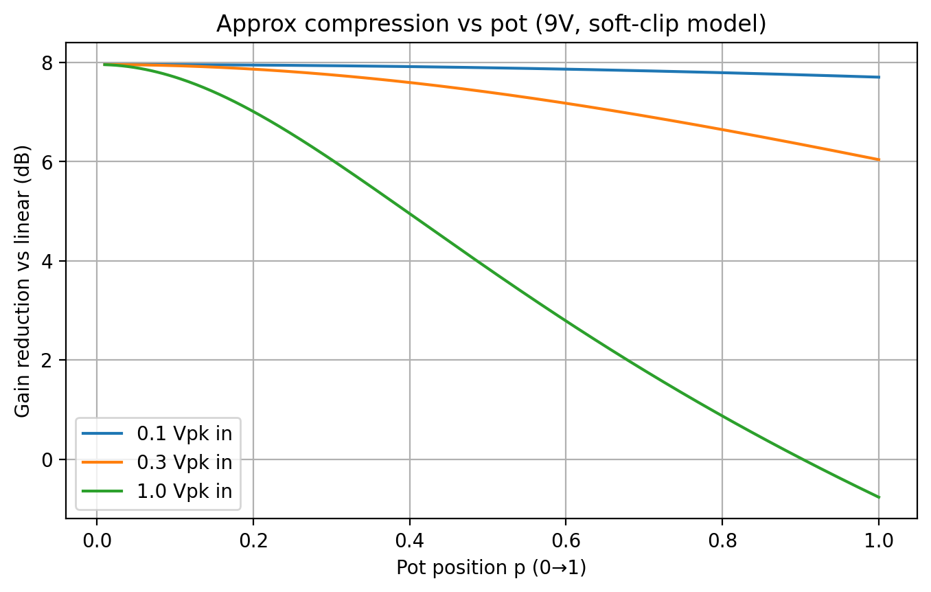
Approximate compression versus pot position
Modeled compression Gain reduction is shown relative to an ideal linear response. A small 0.1 V peak input remains close to linear, while larger 0.3 V and 1.0 V peak signals show progressively more modeled compression as the control is advanced.
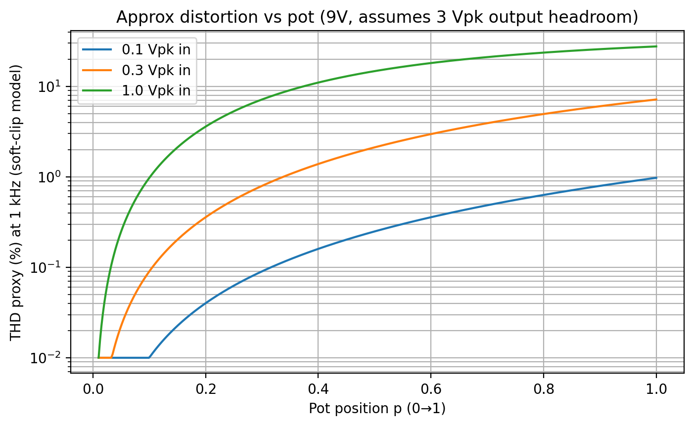
Approximate distortion proxy versus pot position
Distortion proxy This is not a measured THD specification. It is a proxy derived from the same clipping model, illustrating that distortion should rise first for the largest input signals and then increase as gain is turned up.
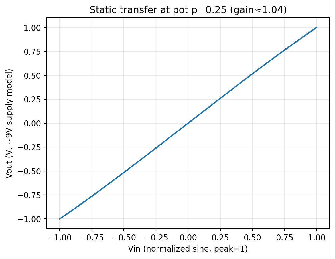
Modeled transfer curve at 25 percent pot position
25% control — gain about 1.04× The transfer curve is essentially straight, representing nearly linear behavior in this model.
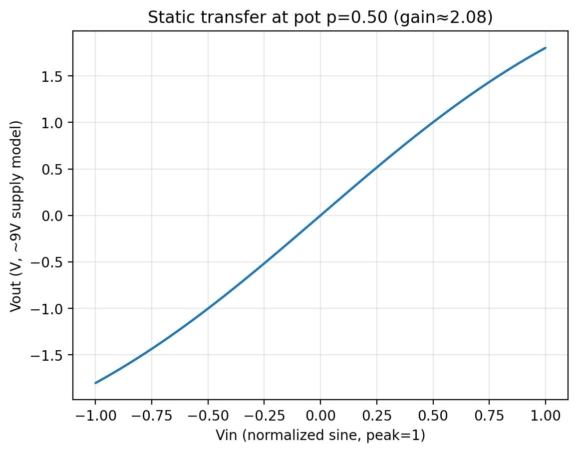
Modeled transfer curve at 50 percent pot position
50% control — gain about 2.08× The ends of the transfer curve begin to bend, showing the modeled onset of soft compression as output headroom is approached.
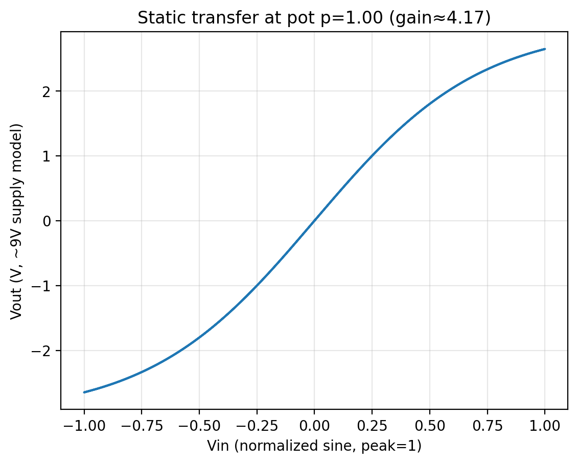
Modeled transfer curve at full pot position
100% control — gain about 4.17× At full modeled boost the curve flattens much more strongly at the extremes, representing substantial modeled compression / saturation for a large input.

Coupling capacitors and the 0.1 µF output capacitor

These graphs show the frequency-dependent behavior of the coupling capacitors and the current demanded by a 0.1 µF capacitor connected at the op-amp output.
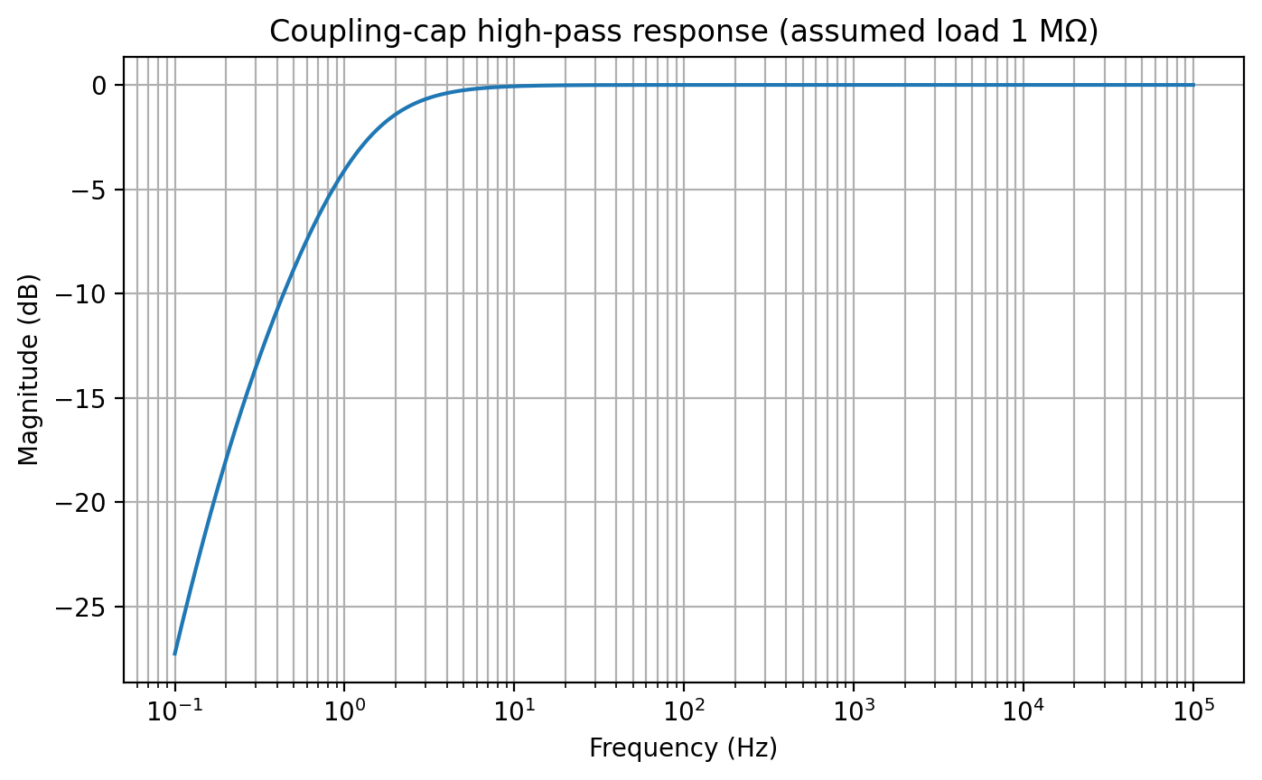
One microfarad coupling capacitor high-pass response with one megohm load
1 µF coupling capacitor with a 1 MΩ load With a very high load resistance, the high-pass corner is far below the guitar audio range. The modeled response is therefore essentially flat through normal audio frequencies.
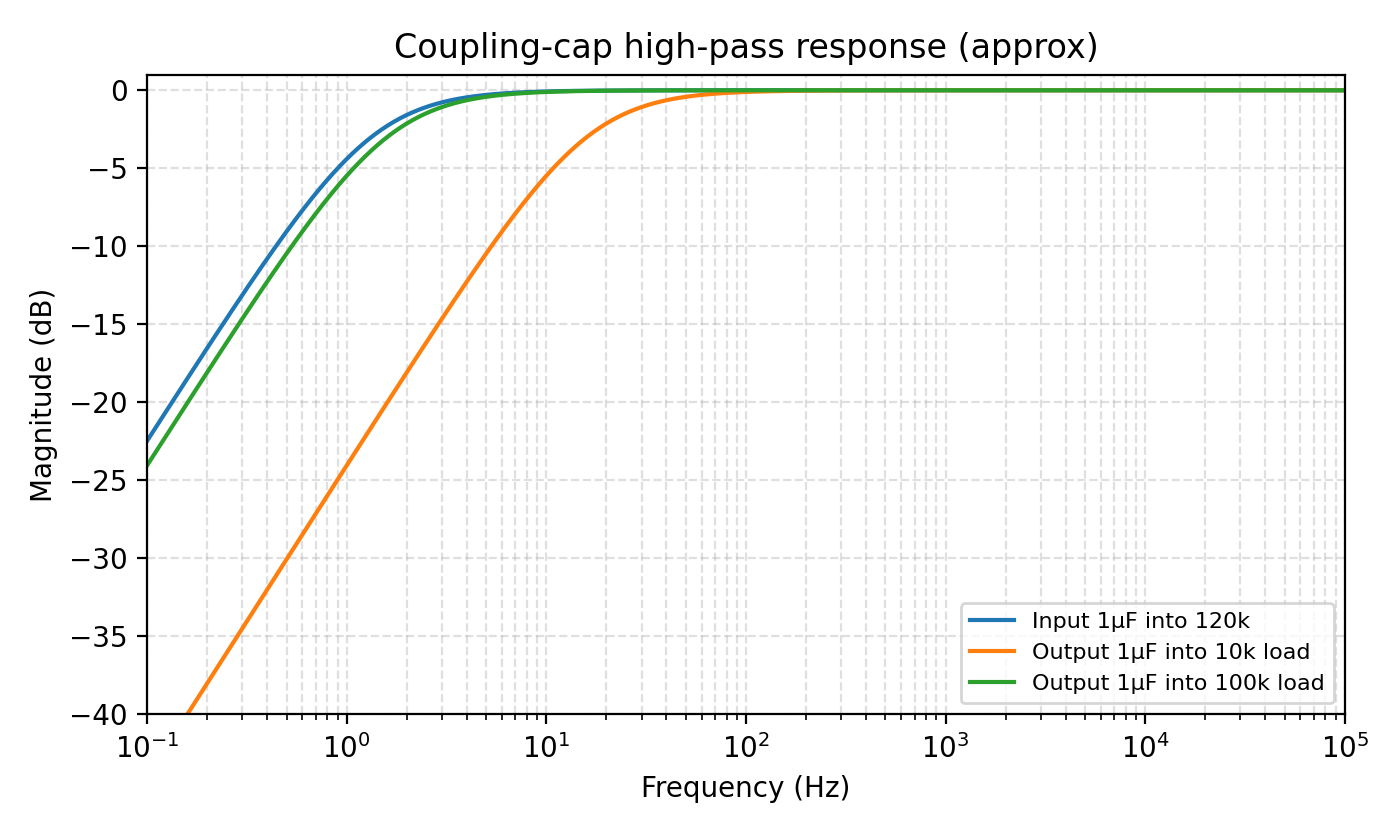
Comparison of coupling capacitor high-pass responses
Coupling capacitor response with different loads The input 1 µF capacitor feeding 120 kΩ has a corner near 1.3 Hz. At the output, 1 µF into 100 kΩ is similarly low at about 1.6 Hz, while a 10 kΩ load raises the corner to roughly 16 Hz and produces the most visible low-frequency roll-off.
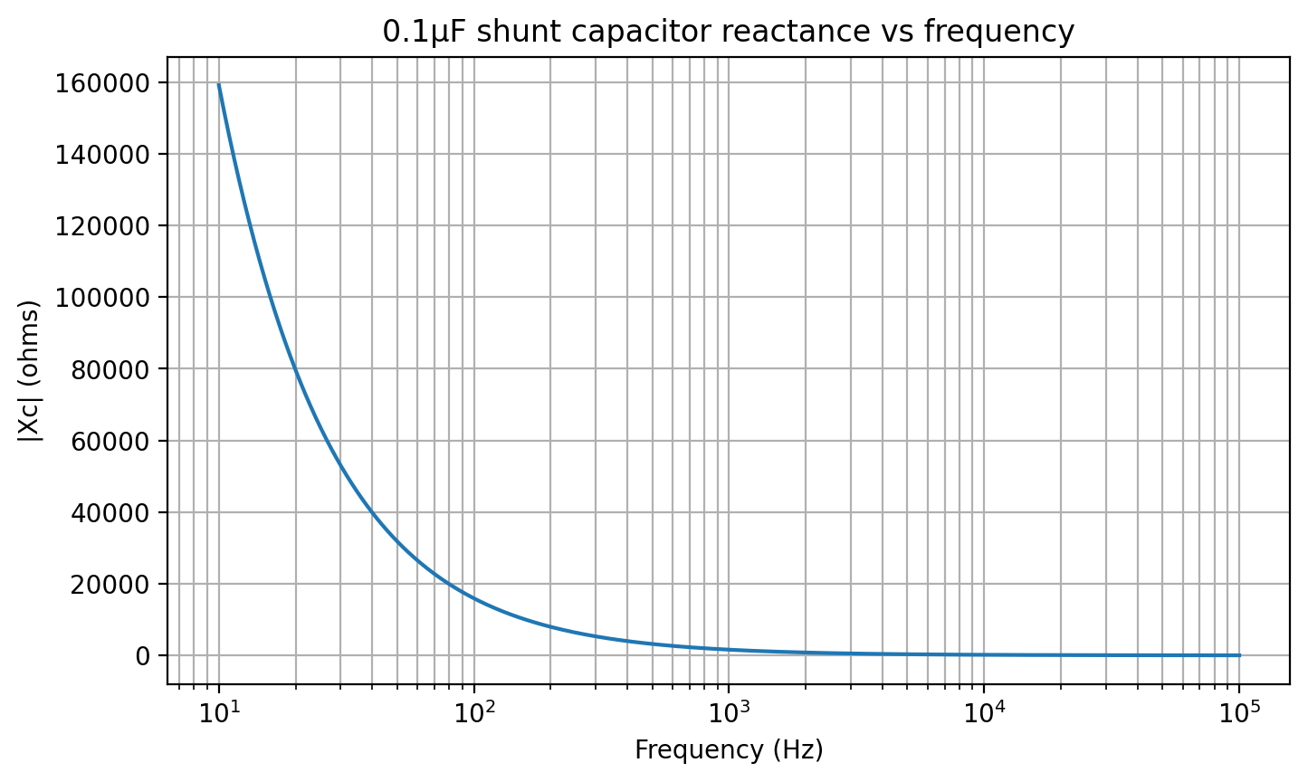
Reactance of 0.1 microfarad output capacitor versus frequency
0.1 µF capacitor reactance versus frequency Capacitive reactance falls as frequency rises. A 0.1 µF capacitor therefore presents a progressively heavier shunt load at high frequencies, which is why its effect becomes much stronger toward the top of and above the audio band.
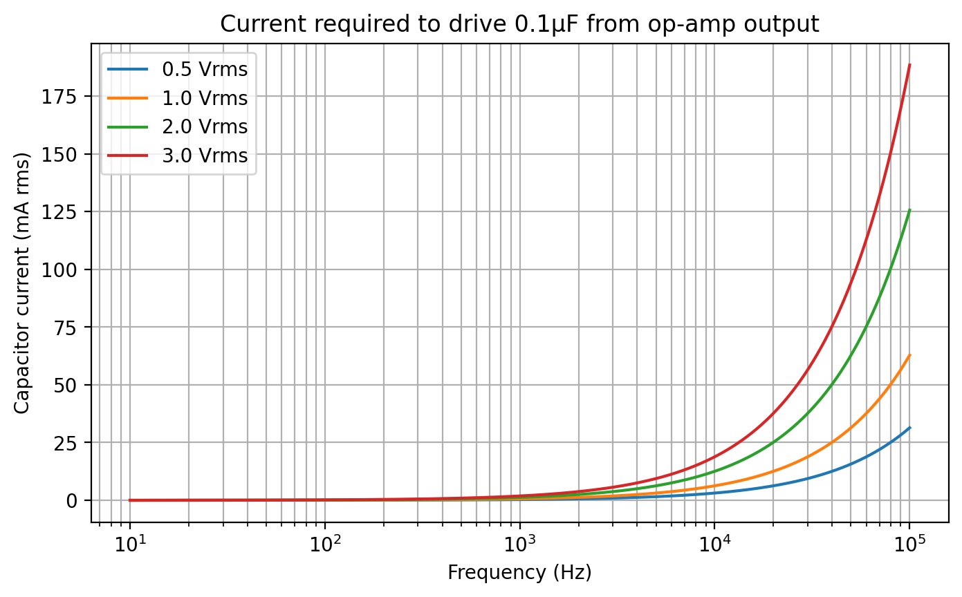
Current required to drive 0.1 microfarad from the op amp output
Current required to drive the 0.1 µF capacitor The required capacitor current rises with both frequency and signal voltage. The curves show that the load becomes increasingly demanding in the upper audio and ultrasonic region, especially at the larger output-voltage levels.

COMPONENT VALUES

Present board component list

ReferenceValue / partFunction
U1NE5534Audio op-amp
R1100 kΩBias network
R2100 kΩBias network
R3120 kΩInput network
C11 µFInput coupling
C20.1 µFBias / decoupling network
C31 µFOutput coupling
C40.1 µFBias / decoupling network
C50.1 µFOutput-stage network
More specifications will be added: measured gain, current draw, frequency response, input/output measurements and other test results can be added here as they are established.

TECHNICAL DOCUMENTS

Datasheets & application notes

Manufacturer documentation used as reference material for the μ-Amp circuit and related experiments.

NE5534 / NE5534A datasheet

Texas Instruments device information, pinout, electrical characteristics and compensation guidance for the NE5534 family.

Open datasheet

Op-amp input-offset nulling

Texas Instruments application report SLOA045 covering methods for trimming operational-amplifier input offset voltage.

Open TI application note